Reference Manual
Protocol
A PDQ stack provides two different channels for data communication apart from the hardware trigger signal. Both SPI and USB can be used to configure the device, write registers and write to memory. The SPI bus provides a read-back mechanism to verify correct communication and read out status. The USB bus is read-only.
Note
Both SPI and USB are active at the same time. They can both be used to access the device. But care should be taken not to use both methods at the same time. In that case SPI has precedence and will interrupt and corrupt any ongoing USB transfers.
Messages
Each communication with the PDQ over SPI or USB forms a message. Each message starts with a one-byte header determining the address of the board to access, the address of the register or memory to access and the action to perform.
| Name | Length (Bits) | Description |
|---|---|---|
adr |
2 | Channel memory or register address |
is_mem |
1 | Flag signaling a channel memory access |
board |
4 | Board address (the selector switch on the PDQ board). 0xf == 15 signaling the broadcast address to access all boards. |
we |
1 | Write-enable. Access is a (register or channel memory) write. |
For example, 0b0_1111_0_00 signals a read from register 0 on any board. Since
data reads can only be performed over SPI and since only one board can drive the MISO line this will read register 0 from the master board.
As another example, 0b1_0011_1_01 signals a write to the second channel memory of board number 3.
The data following the header byte then depends on the action performed. The following table defines the data format both to (MOSI/USB) and from the device:
| Target | Access | MOSI/USB | MISO |
|---|---|---|---|
| Register | read | HEAD dummy dummy |
dummy dummy DATA |
| Register | write | HEAD DATA |
dummy .... |
| Memory | read | HEAD ADDR_LO ADDR_HI dummy dummy .... |
dummy dummy dummy DATA_LO DATA_HI .... |
| Memory | write | HEAD ADDR_LO ADDR_HI DATA0_LO DATA0_HI DATA1_LO DATA1_HI .... |
dummy .... |
Registers
| Name | Register address (adr) |
Description |
|---|---|---|
config |
0 | Configuration register |
crc |
1 | Data checksum register |
frame |
2 | Frame selection register |
Configuration
The configuration register is used to reset the device, configure its clock source, enable and disable it, perform a soft trigger over USB or SPI and to configure the behavior of the AUX/F5 TTL.
| Name | Length (bits) | Description |
|---|---|---|
reset |
1 | Reset the boards. Self-clearing. Reset the FPGA registers. Does not reset memories. Does not reload the bitstream. Does not reset the USB interface. |
clk2x |
1 | Choose the clock speed. Enabling chooses the Digital Clock Manager which doubles the clock and thus operates all FPGA logic and the DACs at 100 MHz. Disabling chooses a 50 MHz sampling and logic clock. The PDQ logic is inherently agnostic to the value of the sample clock. Scaling of coefficients and duration values must be performed on the host. |
enable |
1 | Enable the channel data parsers and spline interpolators. Disabling also aborts parsing of a frame and forces the parser to the frame jump table. Any currently active line will also be aborted. |
trigger |
1 | Soft trigger. Logical or with the hardware trigger. |
aux_miso |
1 | If set, drive the SPI MISO data on the AUX/F5 TTL port of each bord. If cleared, drive the masked logical OR of the DAC channels’ aux data on AUX/F5. |
aux_dac |
3 | Mask for AUX/F5. Each bit represents one channel. |
AUX/F5 is therefore: aux_f5 = aux_miso ? spi_miso : (aux_dac & Cat(_.aux for _ in channels) != 0).
Examples of messages (register writes with header and data):
0b1_1111_0_00 0b000_0_0_0_0_1resets all boards.0b1_0000_0_00 0b000_1_0_1_1_0enables board 0, 100 MHz clock, and MISO on AUX/F5.- The sequence of two configuration register writes
0b1_1111_0_00 0b000_1_1_1_1_0and0b1_1111_0_00 0b000_1_0_1_1_0performs a short trigger over SPI.
Checksum
When receiving message bytes (USB framing and escape bytes are ignored; see below USB Protocol) from either SPI/MOSI or USB, the checksum register is updated with a new value. This can be used to ensure and verify correct data transfer by computing the checksum on the sending end and then reading it back and comparing.
The checksum algorithm used is a 8-bit cyclic redundancy check
(CRC) with a polynomial of 0x07. This polynomial is also commonly known as
CRC-CCITT and implemented both in gateware on the PDQ and in the host side
code. Given some example input it behavoes as follows:
crc8([1,2,3,4,5,6,7,8,9]) == 0x85
The checksum register can be set to initialize it with a known value and read to obtain the current value.
Examples:
0b1_1111_0_01 0x00clears the checksum register on all boards.0b0_1111_0_01 0x00 0x00reads the checksum register on the board connected to MISO.
Frame
The frame selection register determines the currently executed frame for all channels on the addressed board(s). There are currently 32 frames (5 bits) supported. The unused bits are ignored (wrap around on the value) when written and zero when read.
Examples:
0b1_1111_0_10 0x13selects frame 0x13 on all connected boards.
Memory access
The payload data of the message is interpreted as a 16 bit memory address (in the channel memory) followed by a sequence of 16 bit values (two bytes little-endian).
Warning
- No length check or address verification is performed.
- Overflowing the address counter will wrap around to the first address.
- Non-existent or invalid combinations of board address and/or channel number are silently ignored or wrapped.
Examples:
0b1_0001_1_10 0x03 0x04 0x05 0x06 0x07 0x08writes0x0605 0x0807to the memory locations including and following address0x0403of channel0b10on board0b0001.
SPI Protocol
The SPI bus provides access to a stack of PDQ boards over four-wire SPI (separate MISO and MOSI lines).
The SPI bus is wired with CS_N from the SPI master connected to
F2 IN on the master PDQ, CLK connected to F3 IN, MOSI
connected to F4 IN and MISO (optionally) connected to F5 OUT.
F1 TTL Input Trigger remains as waveform trigger input.
Due to hardware constraints, there can only be one board connected to the
core device’s MISO line and therefore there can only be SPI readback
from one board at any time.
Messages on the SPI bus are framed using SPI CS_N. There can be at most one
transaction per SPI CS_N cycle. Register writes are performed when the last
bit of the data is clocked into the device. Register access messages have
fixed length (two bytes for a write and three bytes for a read).
Message data after a register access is ignored.
An implementation of the PDQ SPI protocol is the ARTIQ PDQ driver with its documentation.
USB Protocol
The USB data connection to a PDQ stack is a single, full speed USB, parallel FIFO with byte granularity. On the host this appears as a “character device” or “serial port”. Windows users may need to install the FTDI device drivers available at the FTDI web site and enable “Virtual COM port (VCP) emulation” so the device becomes available as a COM port. Under Linux the drivers are usually already shipped with the distribution and immediately available. Device permissions have to be handled as usual through group membership and udev rules. The USB bus topology or the device serial number can be used to uniquely identify and access a given PDQ stack. The serial number is stored in the FTDI FT245R USB FIFO chip and can be set as described in the old PDQ documentation. The byte order is little-endian (least significant byte first).
Each message on the USB bus is framed by the ASCII STX (0x02) and ASCII
ETX (0x03) control characters. Control characters are escaped using
0xa5. Since the escape character can also appear inside a message each
0xa5 within the message is also escaped using 0xa5.
A valid message as sent over the USB connection therefore looks like:
0xa5 0x02 <escaped-message> 0xa5 0x03
where <escaped message> has all occurences of 0xa5 replaced by 0xa5
0xa5.
Memory Layout
Depending on the bitstream configuration the memory is divided up among the
channels. For three channels the memories contain (16, 12, 12) KiB, for two
channels, they contain (20, 20) KiB and a single channel has all 40 KiB
available.
Overflowing writes wrap around.
The memory is interpreted as consisting of a table of frame start addresses with 8 entries, followed by data.
The layout allows partitioning the waveform memory arbitrarily among the frames of a channel.
The data for frame i is expected to start at memory[memory[i]].
The memory is interpreted as follows (each row is one word of 16 bits):
| Address | Data |
|---|---|
0 |
frame[0].addr |
1 |
frame[1].addr |
| … | … |
frame[0].addr |
frame[0].data[0] |
frame[0].addr + 1 |
frame[0].data[1] |
| … | … |
frame[0].addr + N |
frame[0].data[N] |
| … | … |
frame[1].addr |
frame[1].data[0] |
frame[1].addr + 1 |
frame[1].data[1] |
| … | … |
frame[1].addr + L |
frame[1].data[L] |
| … | … |
Warning
- The memory layout is not enforced or verified.
- If violated, the behavior is undefined.
- Jumping to undefined addresses leads to undefined behavior.
- Jumping to frame numbers that have invalid addresses written into their address location leads to undefined behavior.
Note
This layout can be exploited to rapidly swap frame data between multiple different waveforms (without having to re-upload any data) by only updating the corresponding frame address(es).
Line Format
The frame data consists of a concatenation of lines. Each line has the following format (a row being a word of 16 bits):
header |
duration |
data[0] |
| … |
data[length - 2] |
Warning
- If reading and parsing the next line (including potentially jumping into and out of the frame address table) takes longer than the duration of the current line, the pipeline is stalled and the evolution of the splines is paused until the next line becomes available.
durationmust be positive.
Header
The 16 bits of the header are mapped:
| 15 | 14 | 13 | 12 | 11 | 10 | 9 | 8 | 7 | 6 | 5 | 4 | 3 | 2 | 1 | 0 |
|---|---|---|---|---|---|---|---|---|---|---|---|---|---|---|---|
wait |
clear |
end |
shift |
aux |
silence |
trigger |
typ |
length |
|||||||
The components of the header have the following meaning:
length: The length of the line in 16 bit words including the duration but excluding the header.typ: The output processor that the data is fed into.typ == 0for the DC spline \(a(t)\),typ == 1for the DDS amplitude \(b(t)\) and phase/frequency \(b(t)\) splines.trigger: Wait for trigger assertion before executing this line. The trigger signal is level sensitive. It is the logical OR of the external trigger input and the soft TRIGGER.silence: Disable the DAC sample and synchronization clocks during this line. This lowers the amount of clock feed-through and potentially the noise on the output.aux: Assert the digital auxiliary output during this line. The board’s AUX output is the logical OR of all channelauxvalues.shift: Exponent of the line duration (see Features). The actual duration of a line is thenduration * 2**shift.end: Return to the frame address jump table after parsing this line.clear: Clear the CORDIC phase accumulator upon executing this line. If set, the first phase value output will be exactly the phase offset. Otherwise, the phase output is the current phase plus the difference in phase offsets between this line and the previous line.wait: Wait for trigger assertion before executing the next line.
Warning
- Parsing a line is unaffected by it carrying
trigger. Only the start of the execution of a line is affected by it carryingtrigger. - Parsing the next line is unaffected by the preceding line carrying
wait. Only the start of the execution of the next line is affected by the current line carryingwait.
Spline Data
The interpretation of the sequence of up to 14 data words contained in each
line depends on the typ of spline interpolator targeted by header.typ.
The data is always zero-padded to 14 words.
The assignment of the spline coefficients to the data words is as follows:
typ |
0 | 1 | 2 | 3 | 4 | 5 | 6 | 7 | 8 | 9 | 10 | 11 | 12 | 13 | 14 |
|---|---|---|---|---|---|---|---|---|---|---|---|---|---|---|---|
0 |
a0 |
a1 |
a2 |
a3 |
|||||||||||
1 |
b0 |
b1 |
b2 |
b3 |
c0 |
c1 |
c2 |
||||||||
If the length of a line is shorter than 14 words, the remaining coefficients (or parts of coefficients) are set to zero.
The coefficients can be interpreted as two’s complement signed integers or as unsigned integers depending depending on preference and convenience. The word order is the same as the byte order of the USB protocol: little-endian (least significant word first).
The scaling of the coefficients is as follows:
a0is in units offull_scale/(1 << 16).a1is in units offull_scale/(1 << (32 + shift))/clock_period.a2is in units offull_scale/(1 << (48 + 2*shift))/clock_period**2.a3is in units offull_scale/(1 << (48 + 3*shift))/clock_period**3.b0is in units offull_scale*cordic_gain/(1 << 16).b1is in units offull_scale*cordic_gain/(1 << (32 + shift))/clock_period.b2is in units offull_scale*cordic_gain/(1 << (48 + 2*shift))/clock_period**2.b3is in units offull_scale*cordic_gain/(1 << (48 + 3*shift))/clock_period**3.c0is in units of2*pi/(1 << 16).c1is in units of2*pi/(1 << 32)/clock_period.c2is in units of2*pi/(1 << (48 + shift))/clock_period**2.full_scaleis 20 V.- The step size
full_scale/(1 << 16)is 305 µV.clock_periodis 10 ns or 20 ns depending on theDCMsetting.shiftisheader.shift.2*piis one full phase turn.cordic_gainis 1.64676 (seegateware.cordic).
Note
With the default analog frontend, this means: a0 == 0 corresponds to close to 0 V output, a0 == 0x7fff corresponds to close to 10V output, and a0 == 0x8000 corresponds to close to -10 V output.
Note
There is no correction for DAC or amplifier offsets, reference errors, or DAC scale errors.
Note
Latencies of the CORDIC path, the DC spline path, and the AUX path are not matched. The CORDIC path (both the amplitude and the phase spline) has about 19 clock cycles more latency than the DC spline path. This can be exploited to align the DC spline knot start and the CORDIC output change. DC spline path and AUX path differe by the DAC latency.
Warning
- There is no clipping or saturation.
- When accumulators overflow, they wrap.
- That’s desired for the phase accumulator but will lead to jumps in the DC spline and CORDIC amplitude.
- When the CORDIC amplitude
b0reaches an absolute value of(1 << 15)/cordic_gain, the CORDIC output becomes undefined. - When the sum of the CORDIC output amplitude and the DC spline overflows, the output wraps.
Note
All splines (except the DDS phase) continue evolving even when a line of a different typ is being executed.
All splines (except the DDS phase) stop evolving when the current line has reached its duration and no next line has been read yet or the machinery is waiting for TRIGGER, ARM, or START.
Note
The phase input to the CORDIC the sum of the phase offset c0 and the accumulated phase due to c1 and c2.
The phase accumulator always accumulates at full clock speed, not at the clock speed reduced by shift != 0.
It also never stops or pauses.
This is in intentional contrast to the amplitude, DC spline, and frequency evolution that takes place at the reduced clock speed if shift != 0 and may be paused.
Wavesynth Format
To describe a complete PDQ stack program, the Wavesynth format has been defined.
programis a sequence offrames.
frameis a concatentation ofsegments. Its index in the program determines its frame number.
segmentis a sequence islines. The firstlineshould betriggeredto establish synchronization with external hardware.
lineis a dictionary containing the following fields:
duration: Integer duration in spline evolution steps, in units ofdac_divider*clock_period.dac_divider == 2**header.shifttrigger: Whether to wait for trigger assertion to execute this line.channel_data: Sequence ofspline, one for each channel.
splineis a dictionary containing as key a single spline to be set: eitherbiasorddsand as its value a dictionary ofspline_data.splinehas exactly one key.
spline_datais a dictionary that may contain the following keys:
amplitude: The uncompensated polynomial spline amplitude coefficients. Units are Volts and increasing powers of1/(dac_divider*clock_period)respectively.phase: Phase/Frequency spline coefficients. Only valid if the key forspline_datawasdds. Units are[turns, turns/clock_period, turns/clock_period**2/dac_divider].clear:header.clear.silence:header.silence.
Note
amplitudeandphasespline coefficients can be truncated. Lower order splines are then executed.
Example Wavesynth Program
The following example wavesynth program configures a PDQ stack with a single board, three DAC channels.
It configures a single frame (the first and only) consisting of a single triggered segment with three lines. The total frame duration is 80 cycles. The following waveforms are emitted on the three channels:
- A quadratic smooth pulse in bias amplitude from 0 to 0.8 V and back to zero.
- A cubic smooth step from 1 V to 0.5 V, followed by 40 cycles of constant 0.5 V and then another cubic step down to 0 V.
- A sequence of amplitude shaped pulses with varying phase, frequency, and chirp.
wavesynth_program = [
    [
        {
            "trigger": True,
            "duration": 20,
            "channel_data": [
                {"bias": {"amplitude": [0, 0, 2e-3]}},
                {"bias": {"amplitude": [1, 0, -7.5e-3, 7.5e-4]}},
                {"dds": {
                    "amplitude": [0, 0, 4e-3, 0],
                    "phase": [.25, .025],
                }},
            ],
        },
        {
            "duration": 40,
            "channel_data": [
                {"bias": {"amplitude": [.4, .04, -2e-3]}},
                {"bias": {
                    "amplitude": [.5],
                    "silence": True,
                }},
                {"dds": {
                    "amplitude": [.8, .08, -4e-3, 0],
                    "phase": [.25, .025, .02/40],
                    "clear": True,
                }},
            ],
        },
        {
            "duration": 20,
            "channel_data": [
                {"bias": {"amplitude": [.4, -.04, 2e-3]}},
                {"bias": {"amplitude": [.5, 0, -7.5e-3, 7.5e-4]}},
                {"dds": {
                    "amplitude": [.8, -.08, 4e-3, 0],
                    "phase": [-.25],
                }},
            ],
        },
    ]
]
The following figure compares the output of the three channels as simulated by the artiq.wavesynth.compute_samples.Synthesizer test tool with the output from a full simulation of the PDQ gateware including the host side code, control commands, memory writing, memory parsing, triggering and spline evaluation.
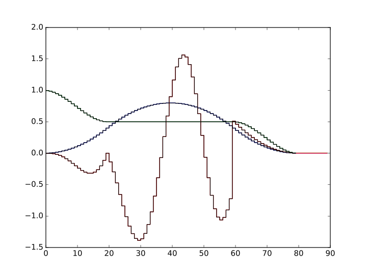
PDQ and Synthesizer outputs for wavesynth test program.
The abcissa is the time in clock cycles, the ordinate is the output voltage of the channel.
The plot consists of six curves, three colored ones from the gateware simulation of the board and three black ones from the Synthesizer verification tool. The colored curves should be masked by the black curves up to integer rounding errors.
The source of this unittest is part of ARTIQ at artiq.test.test_pdq.TestPdq.test_run_plot.